9.4 KiB
9.4 KiB
🌟LilyGo T3 S3 SX1280PA🌟
Overview
- This page introduces the hardware parameters related to
LilyGo T3 S3 SX1280PA
Notes on use
- This version does not have BMS, please use a lithium-ion battery with battery protection function
- Please be sure to connect the antenna before transmitting, otherwise it is easy to damage the RF module
Product
| Product | SOC | Flash | PSRAM |
|---|---|---|---|
| T3-S3 | ESP32-S3FH4R2 | 4MB(Quad-SPI) | 2MB(Quad-SPI) |
PlatformIO Quick Start
- Install Visual Studio Code and Python
- Search for the
PlatformIOplugin in theVisual Studio Codeextension and install it. - After the installation is complete, you need to restart
Visual Studio Code - After restarting
Visual Studio Code, selectFilein the upper left corner ofVisual Studio Code->Open Folder-> select theLilyGo-LoRa-Seriesdirectory - Wait for the installation of third-party dependent libraries to complete
- Click on the
platformio.inifile, and in theplatformiocolumn - Select the board name you want to use in
default_envsand uncomment it. - Uncomment one of the lines
src_dir = xxxxto make sure only one line works , Please note the example comments, indicating what works and what does not. - Click the (✔) symbol in the lower left corner to compile
- Connect the board to the computer USB-C , Micro-USB is used for module firmware upgrade
- Click (→) to upload firmware
- Click (plug symbol) to monitor serial output
- If it cannot be written, or the USB device keeps flashing, please check the FAQ below
Arduino IDE quick start
-
Install Arduino IDE
-
Install Arduino ESP32
-
Copy all folders in the
libdirectory to theSketchbook locationdirectory. How to find the location of your own libraries, please see here- Windows:
C:\Users\{username}\Documents\Arduino - macOS:
/Users/{username}/Documents/Arduino - Linux:
/home/{username}/Arduino
- Windows:
-
Open the corresponding example
- Open the downloaded
LilyGo-LoRa-Series - Open
examples - Select the sample file and open the file ending with
ino
- Open the downloaded
-
On Arduino ISelect the corresponding board in the DE tool project and click on the corresponding option in the list below to select
Name Value Board LilyGo T3-S3 Port Your port USB CDC On Boot Enable CPU Frequency 240MHZ(WiFi) Core Debug Level None USB DFU On Boot Disable Erase All Flash Before Sketch Upload Disable Events Run On Core1 Arduino Runs On Core1 USB Firmware MSC On Boot Disable Partition Scheme Default 4MB with spiffs (1.2MB APP/1.5MB SPIFFS) PSRAM QSPI PSRAM Board Revision* Radio-SX1280PA Upload Mode UART0/Hardware CDC Upload Speed 921600 USB Mode CDC and JTAG Programmer Esptool - Board revision Select according to actual model
-
Upload sketch
📍 Pins Map
| Name | GPIO NUM | Free |
|---|---|---|
| Uart1 TX | 43(External QWIIC Socket) | ✅️ |
| Uart1 RX | 44(External QWIIC Socket) | ✅️ |
| QWIIC Socket IO10* | 10(External QWIIC Socket) | ❌ |
| QWIIC Socket IO21* | 21(External QWIIC Socket) | ❌ |
| SDA | 18 | ❌ |
| SCL | 17 | ❌ |
| OLED(SSD1306) SDA | Share with I2C bus | ❌ |
| OLED(SSD1306) SCL | Share with I2C bus | ❌ |
| SD CS | 13 | ❌ |
| SD MOSI | 11 | ❌ |
| SD MISO | 2 | ❌ |
| SD SCK | 14 | ❌ |
| LoRa(SX1280) SCK | 5 | ❌ |
| LoRa(SX1280) MISO | 3 | ❌ |
| LoRa(SX1280) MOSI | 6 | ❌ |
| LoRa(SX1280) RESET | 8 | ❌ |
| LoRa(SX1280) DIO1 | 9 | ❌ |
| LoRa(SX1280) BUSY | 36 | ❌ |
| LoRa(SX1280) CS | 7 | ❌ |
| LoRa(SX1280) TX | 10 | ❌ |
| LoRa(SX1280) RX | 21 | ❌ |
| Button1 (BOOT) | 0 | ❌ |
| Battery ADC | 1 | ❌ |
| On Board LED | 37 | ❌ |
- QWIIC IO10/IO21 GPIOs are already connected to the Radio TX/RX Pin and cannot be used.
🧑🏼🔧 I2C Devices Address
| Devices | 7-Bit Address | Share Bus |
|---|---|---|
| OLED Display SSD1306 | 0x3C | ✅️ |
⚡ Electrical parameters
| Features | Details |
|---|---|
| 🔗USB-C Input Voltage | 5V |
| ⚡Charge Current | 500mA |
| 🔋Battery Voltage | 3.7V |
Button Description
| Channel | Peripherals |
|---|---|
| BOOT | Boot mode button, customizable |
| RST | Reset button |
LED Description
- CHG LED
| LED State | Details |
|---|---|
| On | Battery charging |
| Off | Battery Full |
| Blink | Battery not connected |
- User LED
- The LED is connected to ESP32 GPIO37, and the LED is turned on or off by writing a high or low level
RF parameters
| Features | Details |
|---|---|
| RF Module | SX1280 |
| Frequency range | 2400 ~ 2500MHz |
| Transfer rate(LoRa) | 0.476 ~ 202 Kbps |
| Transfer rate(FSK) | 0.125 ~ 20000 Kbps |
| Transfer rate(FLRC) | 260 ~ 1300 Kbps |
| Modulation | LoRa 、 FLRC 、 (G)FSK |
WiFi-IPEX
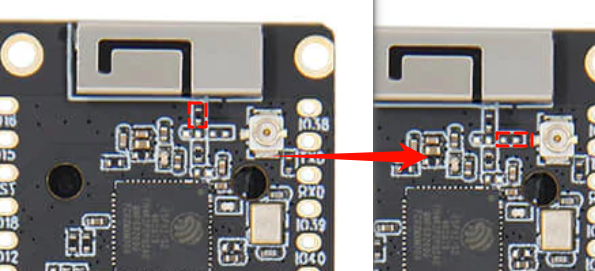
- The following figure shows how to switch the onboard WIFI antenna to IPEX
LoRa-IPEX
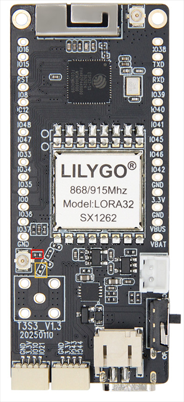
- The following figure shows how to switch the onboard LoRa SMA antenna to IPEX
Frequently asked questions
- When the module turns on PA (transmit) / LNA (receive) data, the module's RX / TX two input pins need to be set. The state truth table is shown in the table below. Setting errors will result in failure to send and receive data normally.
| TX PIN | RX PIN | Radio Status |
|---|---|---|
| 1 | X | PA ( TX active ) |
| 0 | 1 | LNA ( RX active ) |
- Recommended that the software controls the 1280 chip to output 2~5dbm, so that the entire module will output 20dbm power; When the output of the 1280 chip is higher than 2dbm, the output power of the entire module is only 20dbm; When the output of the 1280 chip is higher than 5dbm, the output power of the entire module is only 20dbm, but if 5dbm is given to the FEM, it will damage the FEM chip (the maximum input allowed by the FEM is 5dbm) .If the output of the 1280 chip is lower than 2dbm, the output power of the entire module is within 20dbm.
- SX1280 output power setting cannot be greater than 2~5dbm, otherwise the FEM chip may be damaged. Setting 3dbm already has 20dmb output power